

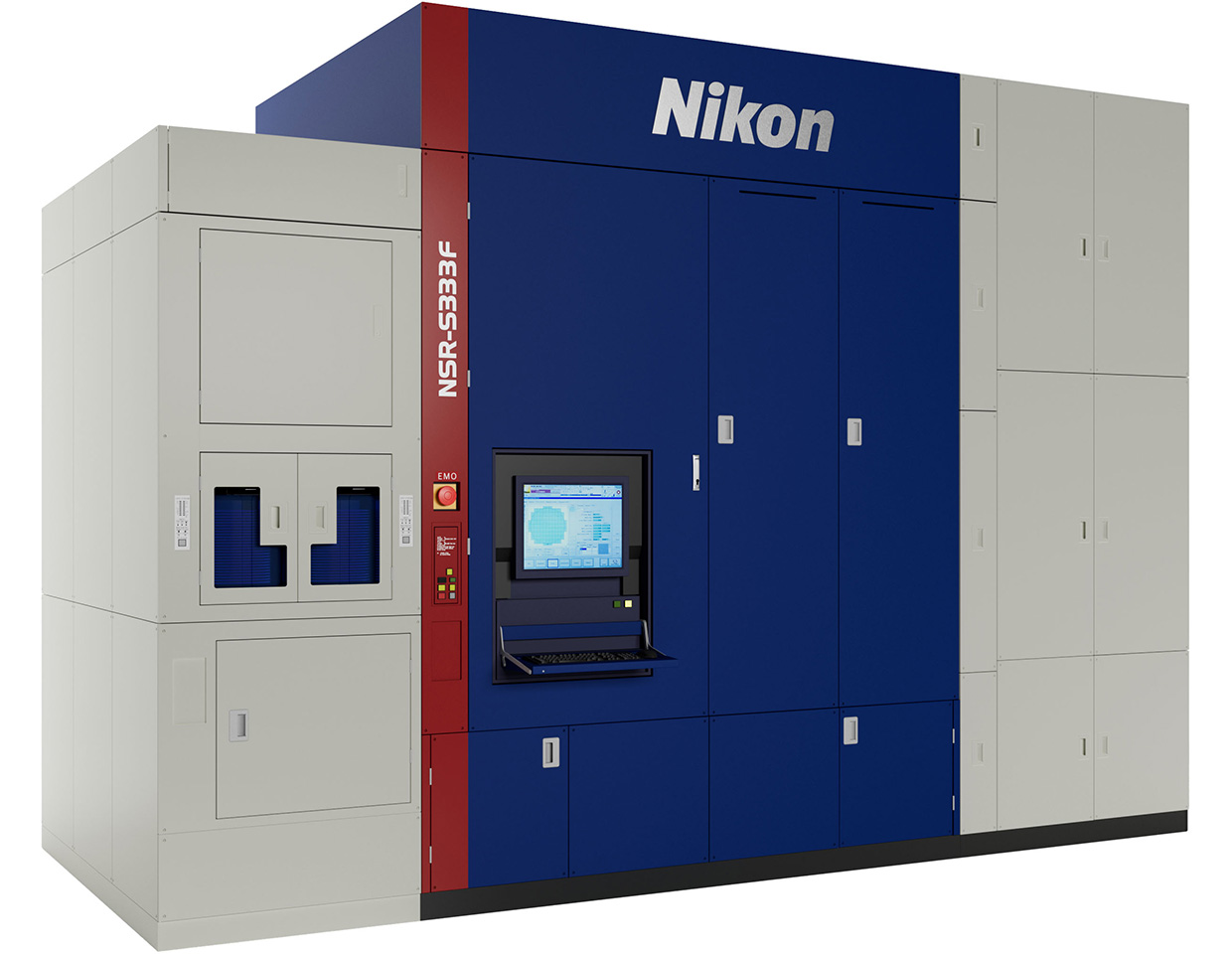
Nikon Corporation has announced the launch of its latest ArF scanner, the NSR-S333F, which combines industry-leading overlay accuracy with exceptional productivity. Building on the advanced platform of its flagship NSR-S636E and refining the proven optics of the NSR-S322F, the new system delivers both precision and efficiency, addressing the growing demands of semiconductor manufacturing. Orders for the NSR-S333F will begin in October 2025, with initial deliveries expected in the second half of 2026.
As the rapid growth of IoT and AI drives demand for smaller, more powerful devices, manufacturers are under pressure to achieve tighter overlay accuracy and faster production. The NSR-S333F responds to these needs by enhancing throughput and overlay performance. With accelerated wafer and reticle stage speeds, the system achieves a throughput of more than 300 wafers per hour, translating into about 1.5 times higher productivity than its predecessor. At the same time, it introduces significant advances in wafer alignment measurement, reticle stage measurement, and autofocus, resulting in an overlay accuracy of less than or equal to 4 nanometers — the best among ArF scanners announced to date.
With a resolution of 65 nm and stability, the NSR-S333F sets a new benchmark in semiconductor lithography technology.


Leave a comment